Metamaterial/ Metasurface absorbers
In the previous post about classical perfect light absorbers, we discussed the thin film based absorbers in the shape of Salisbury screen absorbers and Jaumann absorbers. Now, these thin film based absorbers, especially the Salisbury screen, can be titled as an early demonstration of metasurface absorbers as it involves using a top thin film of subwavelength thickness, and usually, the height of the entire structure is less than the operating wavelength. The latest demonstrations of metamaterial/metasurface absorbers usually include three layers with Metal–Dielectric–Metal (MDM) configuration. The top metal layer is nanostructures, which reduces the reflection and allows maximum transmission of light towards the dielectric layer. The middle dielectric layer traps the light between two metal layers. The bottom metal layer is made thick in order to avoid transmission from the entire absorber. The bottom metal layer can only reflect the light.
Resonant absorbers/ Resonators/ Narrowband absorbers
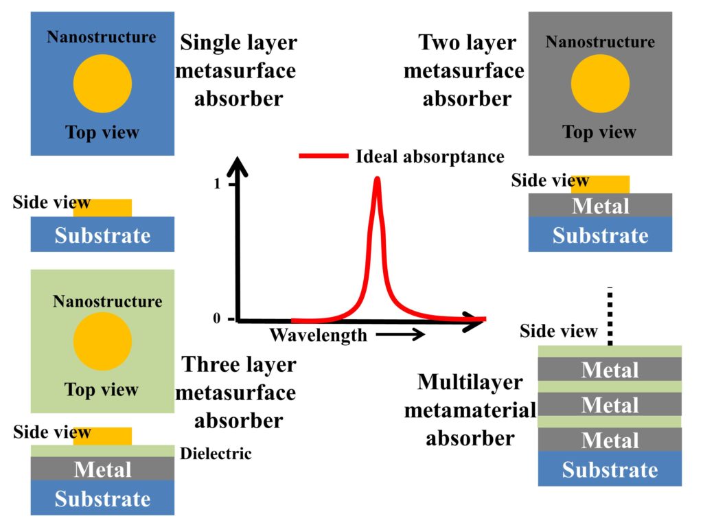
The resonant metamaterial/ metasurface absorbers are electromagnetic (EM) wave absorbers that give a narrowband absorptance spectrum, and that is why they are also referred to as narrowband absorbers. These types of absorbers are particularly suitable for the application of filtering, sensing, and emission. The design of these absorbers is variable depending upon the targetted application. These absorbers can either be single-layered, or multilayered with or without nanostructures. The single-layered absorbers usually have a bottom substrate layer and on top of the substrate, there is nanostructured metal or semiconductor material layer. Similarly, a two-layer design can have a metal layer at the bottom and a nanostructured layer on top. The three-layered absorber design will follow the MDM design with a nanostructured layer on top. Depending upon the thicknesses of the layer, this absorber can either be metamaterial absorbers or metasurface absorbers (if we consider the thickness to be much smaller than the operational wavelength). The metasurface narrowband absorbers up to three layers and metamaterial multilayered narrowband absorbers are shown in Fig. 1 with their ideal absorptance curve.
Broadband absorbers
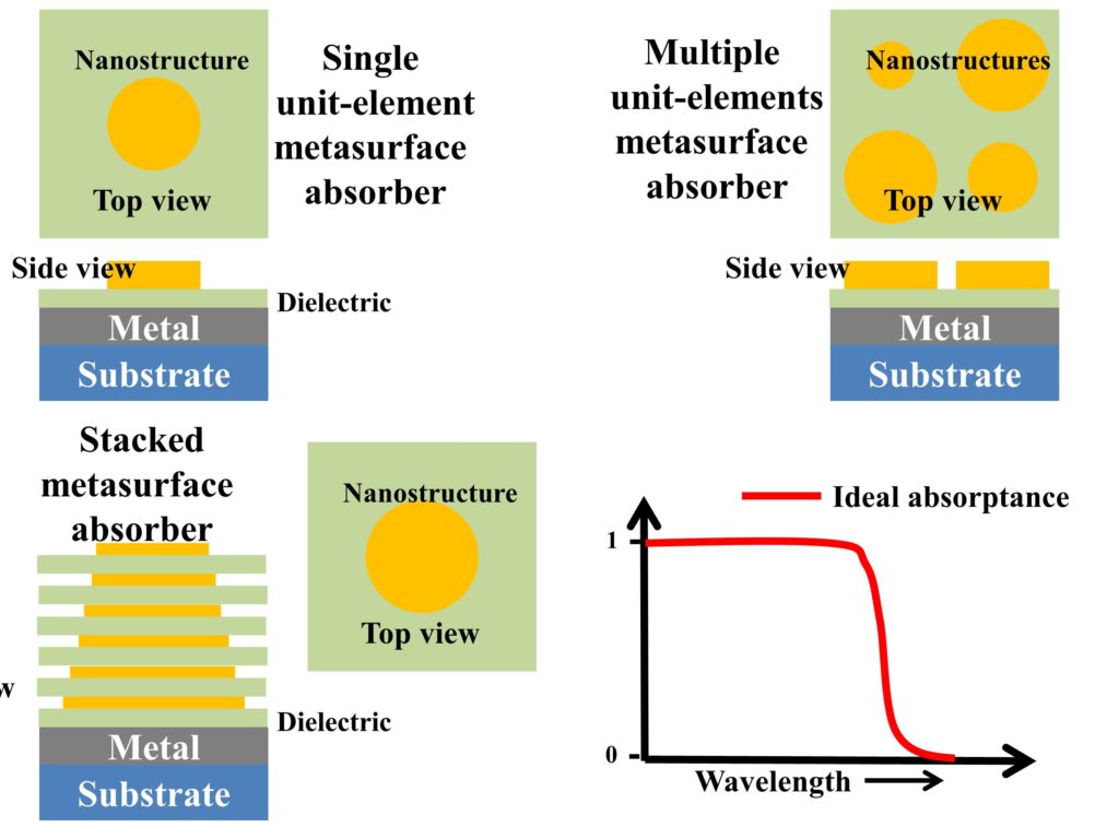
The broadband metamaterial/ metasurface absorbers give a wideband absorptance spectrum. The broadband absorber can also have different designs depending upon the targetted application. These absorbers can also be single-layered, or multilayered with or without nanostructures. They follow almost all the designs of narrowband absorbers, but they can also be made by making stacks of the narrowband metamaterial and metasurface absorbers. By employing stacks, the height dimension of the design can increase, and therefore, metamaterial will be achieved rather than a metasurface. A way of limiting the height dimension and keeping the design constrained to add multiple nanostructured units on top, which can present their separate resonances. These resonances are then designed to overlap on each other such that the metasurface absorber yields broadband response. The stacking has an inherent issue of alignment (keep the stacks exactly on top of each other), which reduces its efficiency. Therefore, increasing the number of unit elements of nanostructures is the primary design configuration for broadband absorbers. Single unit elements can also yield broadband response in the visible regime if their designs are optimized. Since the designs are dependent on material properties, there is a limitation to which a broadband response can be attained from a single unit element. The single unit-element metasurface broadband absorbers, multiple unit-element metasurface broadband absorbers, and stacked metamaterial broadband absorbers are shown in Fig. 2 with their ideal absorptance curve.