
Introduction to MOSFETs
Mohamed M. Atalla worked at Bell Labs in the late 1950s on the issue of surface states, which he discovered. He carried on Frosch’s oxidation research, attempting to passivate the surface of silicon by generating an oxide layer on top of it. He felt that growing a very thin layer of high-quality thermally generated SiO2 on top of a clean silicon wafer would neutralize surface states enough to enable the creation of a working field-effect transistor.
In 1957, he recorded his findings in his BTL notes, and the following year, in 1958, he presented his findings at an Electrochemical Society meeting. This was a big step forward since it allowed MOS technology to be combined with silicon integrated circuit (IC) chip technology. The next year, John L. Moll published his description of the metal–oxide–semiconductor (MOS) capacitor at Stanford University.
J.R. Ligenza and W.G. Spitzer, Atalla’s collaborators who studied the mechanism of thermally generated oxides, were able to construct a high-quality Si/SiO2 stack, which Atalla and Kahng subsequently utilized to illustrate the efficacy of their study. Mohamed Atalla and Dawon Kahng successfully created a working metal–oxide–semiconductor field–effect transistor (MOSFET) device in November 1959, marking the beginning of the MOSFET’s development. The device is covered by two patents, both of which were filed separately in March 1960 and cover the same invention by Atalla and Kahng. The researchers presented their results at Carnegie Mellon University’s Solid-State Device Conference in June 1960. In the same year, Atalla argued for the use of MOSFETs to build MOS integrated circuit (MOS IC) chips, highlighting the ease with which MOSFETs could be fabricated. BJT, MOSFET, IGBT, SCR, TRIAC, and other similar power electronic switching components are critical components used in the building of a wide range of circuits, from simple driver circuits to complex power rectifiers and inverters, among other uses. The most basic amongst them all is the BJT. MOSFETs, second only to bipolar junction transistors, are the most widely utilized power switches. MOSFETs, as opposed to bipolar transistors, can withstand greater voltages and currents, making them ideal for high-power applications.
Design of metal–oxide–semiconductor field–effect transistor (MOSFET)
MOSFETs are semiconductor devices that have a metal gate that is isolated from the conductive channel between the drain and source contacts by a very thin oxide-based insulating layer. Depending on the value of the gate voltage, a field is created that allows or blocks current flow. In contrast to a JFET, which uses a p-n junction to control the channel, and a MESFET, which uses a metal-semiconductor (Schottky) junction to control the channel.” “Because MOSFETs are available at such small sizes, they may be used as either a core or an integrated circuit, in which case they are designed and manufactured on a single silicon chip. The area of switching in electronics has seen a considerable revolution because of the creation of the MOSFET device.
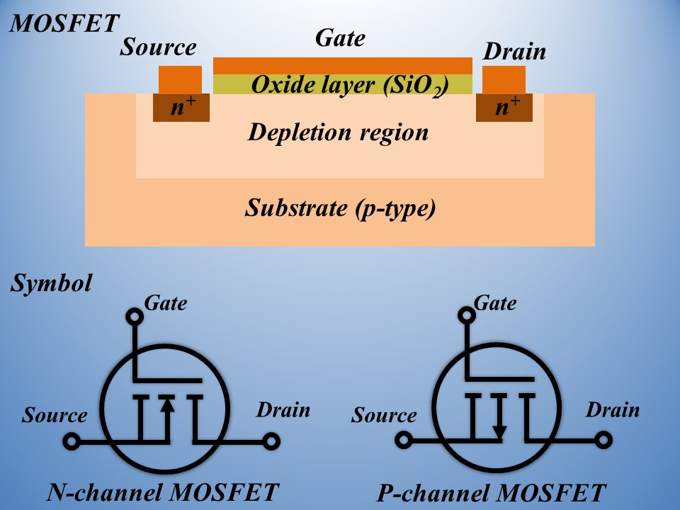
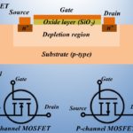
A MOSFET is a four-terminal device with four terminals: the source (S), the gate (G), the drain (D), and the body (B)”. “MOSFETs are three-terminal devices, and the body of a MOSFET is connected to the source terminal, creating a device like a field-effect transistor in appearance as shown in Fig. 1. MOSFET is commonly regarded as a kind of transistor and is used in both analog and digital circuits, depending on the application.
Operation of MOSFETs
The operation of a MOSFET is based on the electrical fluctuations that occur in the channel width, as well as the passage of carriers, according to the above-mentioned metal-oxide-semiconductor field-effect transistors construction (either holes or electrons). The source terminal is where charge carriers enter the channel, while the drain terminal is where they exit.
The voltage supplied to an electrode known as the gate, which is located between the source and the drain and regulates the channel width, controls the channel width. A very thin covering of metal oxide in the area protects it from the channel. The MOS capacity is present in the device, and it is this region that is crucial since the device’s whole operation is reliant on it.
Working principle
It is feasible to control both the voltage and current flow between the source and drain terminals using the MOSFET device’s fundamental design principle. It functions as a switch, and the device’s functioning is controlled by the MOS capacitor. A MOSFET’s most critical component is the MOS capacitor.
It is feasible to transform the p-type semiconductor surface beneath the oxide layer positioned between the source and drain terminals to an n-type semiconductor surface by using gate voltages of either positive or negative magnitude (see figure). The holes beneath the oxide layer are pushed downward with the substrate when a repulsive force is applied to the positive gate voltage, resulting in a negative gate voltage.
The bonded negative charges coupled to the acceptor atoms occupy the depletion zone, which is bordered by positive charges. When electrons are present, it is feasible to build a channel. The positive voltage also pulls electrons from the n+ source and drain regions, which the positive voltage subsequently draws into the channel. When a negative voltage is applied instead of a positive voltage, a hole channel is formed underneath the oxide layer.
Applications of metal-oxide-semiconductor field-effect transistors
The following are some of the most significant uses of metal-oxide-semiconductor field-effect transistors (MOSFETs).
- MOSFETs are electronic devices that are utilized for switching and amplifying electronic signals in electronic devices.
- It is utilized as an inverter in a variety of applications.
- It has the potential to be employed in digital circuits.
- A MOSFET may be used as a high-frequency amplifier in certain situations.
- Resistance, capacitor, and inductor are all examples of passive elements that may be employed with it.
- It may be employed in the driving of brushless direct current motors.
- It is suitable for usage in electronic DC relays.
It is used in the switch mode power supply system (SMPS).
Further readings
If you liked this post you might be interested in reading the following posts.
- Laser and its applications in medicine and technology
- Birefringence and birefringent materials
- Blackbody radiation calculator for specific wavelengths and temperatures
- Light Emitting Diodes (LEDs), their design and applications
- Design of MOSFETs, their working, and applications
- Construction, working, and new technologies of OLED TV
- Laser and its applications in medicine and technology
- LED light, its construction, types and colors, power, life, and technology
- Optical fiber design and applications
- Radiation therapy for cancer treatment and its side effects
- X-ray Imaging: What are X-rays and how are X-ray images taken?
- Scattering of light and its different types
- The achromatic lens to remove chromatic aberration
- Wave plates and polarizers for polarization manipulation
- Birefringence and birefringent materials
- Demystifying Solar Panel Specifications: Your Guide
- Construction, working, and new technologies of OLED TV
- LED light, its construction, types and colors, power, life, and technology
- Latest Trends And Development In Solar Technology
- Geothermal energy and its advantages
- Solar tracker to increase the efficiency of solar energy systems
- Solar tree for compact energy collection
- Water pumping system design calculator using solar energy
- Effective harnessing solar energy through spray-on solar cells
- Are perovskite solar cells future of solar energy harvesting?
This really answered my problem, thanks!
very good post, i actually love this web site, keep on it
I appreciate your focus on the challenges and opportunities presented by the gig economy.
excellent put up, very informative. I ponder why the other specialists of this sector do not realize this. You must proceed your writing. I am confident, you’ve a great readers’ base already!