
Introduction to Light Emitting Diodes (LEDs)
All semiconductor diodes available today are used in some capacity, but LEDs are the most widely used of them all. The visible light or the invisible infrared light of a light-producing diode may be transmitted one-sidedly (biased). There are several uses for LEDs that don’t emit any visible light, such as controllers. A light-emitting diode (LED) is an optical semiconductor device that produces a light beam when power is applied. Using LED, you can convert electrical energy into light. Free electrons in the conduction band mix with holes in the valence band and produce light when the Light Emitting Diode (LED) is forward one-sided.
The LED’s semiconductor internal structural material contains electrons and holes, both of which interact with each other. The LED’s photons’ energy is determined by the groups’ separation. Because the photon energy takes up the repetition and tone of the transmitted light, light emitted by semiconductors with varying band holes may be seen in a variety of colors. Changes to the dynamic district, or light-radiating district, may be made to alter the specific repeat (hiding). – Compound semiconductor materials are used to make LEDs, and these materials are found in the irregular table’s pack III and get-together V. Gallium arsenide (GaAs) and gallium phosphide (GaP) are two examples of III-V materials often utilized in LEDs (GaP). There were no blue and white LEDs until the mid-90s when LEDs began to expand their range of tones. GaN-based LEDs have completed the range of tones and opened up a wide range of new applications as a result of their advancement. There is just one path for an electric current to go through a typical p-n convergence diode. Electricity can flow forward when the bias is forward, but it cannot flow backward when the bias is reversed. p-n crossing point diodes only function in forwarding inclination.
LEDs and P-n crossing point diodes both need a forward inclination to operate properly. If you want to construct an LED, you need to connect the n-type material to the battery’s neutral terminal and the p-type material to the positive terminal. The n-type material should be charged in the opposite direction, and the p-type material should be fully charged by the end of the day. Instead of silicon or germanium, gallium, phosphorus, and arsenic elements are utilized to advance LEDs instead of the traditional p-n crossing point diode. Silicon is the most frequent material used in p-n junction diodes because it is less sensitive to temperature. Furthermore, it permits the flow of electricity without causing any harm. Every now and again, diodes are made out of germanium. However, diodes made of silicon or germanium do not emit light. They produce heat as a means of releasing energy. As a result, LEDs don’t need silicon or germanium as component materials. It is the energy band opening of the semiconductors that determines how many times the light will recur in the system. As a result of their good optical coatings and sloppy form, these materials are believed to be able to effectively exude light in the devices.
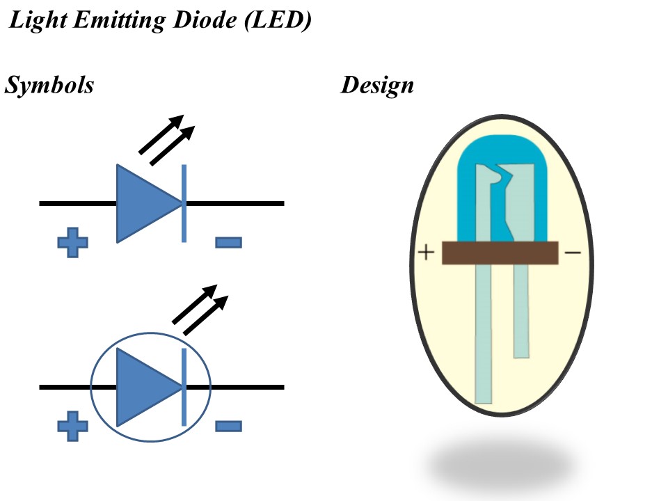
The symbol and design of Light Emitting Diode (LED) is shown in figure 1 below.
Early History of Light Emitting Diodes
Electroluminescence is the name given to the process in which light is emitted as a result of an electric field or current. A gem of silicon carbide and a feline’s stubble finder was used by the English scientist H. J. Round of Marconi Labs in 1907 to discover the uniqueness of electroluminescence as a phenomenon. In 1936, Georges Destriau discovered that an exchanging electrical field might offer electroluminescence when zinc sulfide (ZnS) powder was suspended in an encasing. In 1939, Hungarian Zoltán Bay and György Szigeti licensed a lighting device based on SiC, with a choice of boron carbide that radiated white, yellowish-white, or greenish-white depending on impurities present, preempting LED lighting in Hungary. Using an apparatus using SiC gems and a current wellspring of a battery or a heartbeat generator, Kurt Lehovec, Carl Accardo, and Edward Jamgochian explained the first LEDs in 1951. In 1953, they used a correlation with a variation, pure, gem to further their understanding. J. W. Allen and R. J. Cherry presented the first red visible-spectrum LED towards the end of 1961.
Raw materials and efficacy of Light Emitting Diodes (LEDs)
All three types of gallium phosphide (GaP) or arsenide phosphide are utilized in the production of LED lighting fixtures. A GaP is a most often used kind (GaAsP). LEDs with various substrates and contaminations provide varying levels of light concealment. Unrefined elements are included later in the collection structure; rather than defects, they ensure that the LED operates perfectly. It is this process is referred to as doping. Typically, defilements like Zinc or nitrogen are utilized, although other elements including silicon, germanium, and tellurium have been used as well. As of right now, the LED will serve as an electrical device by supplying direct power to the semiconductor. To create a layer with excess or shortfall of electrons, poisons must be used.
It is essential to transfer capacity to and from the device in order for it to be complete. As a result, the substrate should be equipped with wires. It is essential that these wires adhere well to the semiconductor and are capable of withstanding the stresses that may be applied to them due to such processes as heating and cooling. Gold and silver alloys are the most often utilized because they form a strong connection with gallium on the wafer’s outer layer. Rather like Lucite paperweights, the LEDs are wrapped in a translucent plastic shell. A variety of plastics may be used for the LED, and its optical qualities will determine how the light appears after it has faded. Diffusive polymers allow light to be scattered in a variety of ways. It is possible to design the transparent ones such that light from an LED may shine directly out of them in a restricted bar. Plastics may be tinted to enable the light of a particular hue to pass through, changing the LED’s color.
As with its radiant adequacy, light discharging’s rating has yet to be established. Generally, it is measured in lumens per watts, which is the amount of dazzling advancement that the diode receives from the electrical information power it receives. The eye’s reaction to various wavelengths of light is influenced by the radiant movement.
| Color | Wavelength (nm) | Typical efficacy (LM/W) | Typical efficacy (W/W) |
| Red | 620-645 | 72 | 0.39 |
| Green | 520-550 | 93 | 0.15 |
| Blue | 460-490 | 37 | 0.35 |
| Cyan | 490-520 | 75 | 0.26 |
| Red-Orange | 610-620 | 98 | 0.29 |
Layers in LEDs
The p-type semiconductor, the n-type semiconductor, and the Depletion layer make up an LED. A depletion layer separates the p-type semiconductor from the n-type semiconductor.
P-type semiconductor
A p-type semiconductor is defined as the result of the addition of trivalent impurities to a standard or pure semiconductor. Free electrons make up the majority of charge transporters in a p-type semiconductor, with holes making up the majority of charge transporters. Similarly, in a p-type semiconductor, holes carry the vast majority of the electric current.
N-type semiconductor
An n-type semiconductor is created as soon as pentavalent cations contaminate the natural semiconductor. The majority of charge carriers in n-type semiconductors are free electrons, whereas the remaining charge carriers are holes. As a result, in an n-type semiconductor, unbound electrons carry the majority of the electric current.
Depletion layer or region
An area known as a depletion area is located between the p-type and n-type semiconductors and is devoid of adaptive charge carriers (free electrons and holes). This area serves as a barrier to the flow of electricity, and it’s incompatible with the electron and hole streams produced by n-type and p-type semiconductors, respectively.
Working of an LED
For LEDs to function, they must be placed in an upright posture. At this point, free electrons and holes on either side of an LED are driven toward each other, resulting in an equitable distribution of electrons and holes. Only at the crossing point or depletion zone, electrons become free again, recombining with holes in positively charged particles. Because protons have more electrons, we know that positive particles have less. They can now recognize the electrons. Depletion regions are filled with free electrons and holes.
A little distance away in the depletion area, p-side holes and electrons recombine due to free electrons and holes in the depletion district recombination. As a result, the p-n intersection will increase the number of charge transporters. Before recombining in the utilization region, charge transporters from p and n sides will pass via the p-n junction. For example, free electrons from an n-type semiconductor may cross the p-n intersection and join with holes in p-type semiconductors. N-type semiconductor free electrons join with holes that have traveled via p-n crossings from the p-type semiconductor. Hence, in the usage zone, recombination takes place similarly as in p- and n-type semiconductors. Recombination takes place. A tiny amount of energy is released as visible light when electrons in the conduction band break free and recombine with holes in the valence band.
Most of the energy is transferred as heat in silicon and germanium diodes, whereas the amount of light that is emitted is little. No matter what, the emitted photons in materials like gallium arsenide and gallium phosphide are sufficiently energetic for a shockingly noticeable light to occur.
Construction of an LED
Light Emitting Diodes (LEDs) are designed and developed in a completely different way than a typical semiconductor signal diode. When the LED’s PN junction is one-sided in the direction of forwarding travel, it will emit light. The PN junction is shielded from barometrical disturbing effects, vibrations, and heated shock by an epoxy tar hemispherical formed shell body. These materials include Gallium Arsenide, Gallium Arsenide Phosphide, Gallium Phosphide, Gallium Arsenide Phosphide, Gallium Phosphate, Aluminum Gallium Nitride, Silicon Carbide, and so on. The domed top of the LED acts as a point of convergence that shines the most significant proportion of light, even though the LED convergence itself doesn’t produce much light, so the epoxy sap body is verifiable in such a way that the light photons sent by the convergence are reflected away from the substrate base and captured.
Avocation is why the transmitted light looks usually superb at the highest level of LED. Red-tinted Light Emitting Diodes often need a Gallium Arsenide substrate, while green, yellow, and orange-tinted Light Emitting Diodes are rare on Gallium Phosphide substrates. The N-type layer is doped with Tellurium (Te), while the P-type layer is doped with Zinc for red concealing outflow. Separate aluminum and aluminum tin layers are used to create the contact layers on the P and N sides, respectively. Three semiconductor layers are stored on the substrate during the LED assembly process as one of the methods. The n-type semiconductor, p-type semiconductor, and dynamic area saved the substrate money. In the n-type and p-type semiconductor layers, the dynamic area is accessible.
LED characteristics and applications
One-sided forward conduction causes an increase in current, which may be managed in order to prevent the device from being destroyed. Using a fiber optic connection, an undistorted signal may be sent since the light result is precisely proportional to the current inside its dynamic locality.
Applications of light emitting diodes
- Used as a source of light for televisions.
- Displayed in exhibits
- In the future, remote controllers will be able t
- Involved in the manufacturing of automobiles
- The dimming of lights is made possible by LEDs
- automobiles with engines and bicycles with light
- Indicators, signs, and signals for traffic
- display of data on bulletin boards
- uses in medicine and playthings
- a few additional lights
Advantages and disadvantages of utilizing LEDs
Advantages
- Small chip size and low cost, as well as long life
- Low temperature and high energy efficiency
- Plan flexibility and a wide range of hues
- Eco-friendly and high-speed exchange
- Enhanced luminosity
- Intentionally focused and less vulnerable to harms
- Less heat is being transmitted.
- Warm stun and vibrations have less effect on them.
- There are no UV rays present.
Disadvantages
- Radiant power and frequency of the LED are dependent on the surrounding temperature. An overabundance of voltage or a potential overabundance of current can harm a person who is susceptible to it.
- Anecdotally, productivity can only be attained in unusually cool or beat conditions.
Further readings
If you liked this post, you might be interested in reading the following posts.
- Laser and its applications in medicine and technology
- Birefringence and birefringent materials

- Blackbody radiation calculator for specific wavelengths and temperatures
- Light Emitting Diodes (LEDs), their design and applications
- Design of MOSFETs, their working, and applications
- Demystifying Solar Panel Specifications: Your Guide
- Construction, working, and new technologies of OLED TV
- LED light, its construction, types and colors, power, life, and technology
- Latest Trends And Development In Solar Technology
- Geothermal energy and its advantages
- Solar tracker to increase the efficiency of solar energy systems
- Solar tree for compact energy collection
- Water pumping system design calculator using solar energy
- Effective harnessing solar energy through spray-on solar cells
- Are perovskite solar cells future of solar energy harvesting?
- Construction, working, and new technologies of OLED TV
- Laser and its applications in medicine and technology
- LED light, its construction, types and colors, power, life, and technology
- Optical fiber design and applications
- Radiation therapy for cancer treatment and its side effects
- X-ray Imaging: What are X-rays and how are X-ray images taken?
- Scattering of light and its different types
- The achromatic lens to remove chromatic aberration
- Wave plates and polarizers for polarization manipulation
- Birefringence and birefringent materials