
The prime objective of this post is to get familiar with bipolar junction transistor (BJT) and its related terminology. The primary purpose of a BJT is to amplify the current. This allows BJTs to be utilized as amplifiers or switches in electronic devices such as cell phones, industrial control, television, and radio transmitters. NPN (a BJT made from n-type, p-type, and n-type semiconductors) and PNP (a BJT made from p-type, n-type, and p-type semiconductors) are the two different types of BJTs that are available in the market.
Introduction to bipolar junction transistors (BJTs)
The bipolar junction transistor (BJT) was invented in the early 1950s and transformed the world of electronics. Computer memory, microprocessors, and other integrated circuits are built on transistors. It has three terminals emitter, base, and collector, which are labeled E, B, and C, respectively.
There are two PN junctions in this transistor. A PN junction is formed when n-type and p-type materials are joined together. Due to the diffusion of holes from the p-type region and diffusion of electrons from the n-type region to the p-side, an electrostatic region of just charges is left at the junction where p-type and n-type materials are joined. This junction stops further diffusion of electrons and holes.
The emitter-base junction is a PN junction that exists between the emitter and the base, while the collector-base junction is a PN junction that exists between the collector and the base. The collector-base junction is reverse biased, while the emitter-base junction is forward biased.
BJTs were originally built of germanium, but more contemporary transistors are made of silicon. NPN transistors and PNP transistors are the two varieties of BJTs. It is a bipolar device in which both charge carriers, namely electrons and holes, conduct. In the base region, the number of electrons diffused is greater than the number of holes diffused in the emitter region. In the base area, electrons act as a minority carrier if the transistor we take is of n-p-n configuration (discussed in the next section).
Types of BJTs
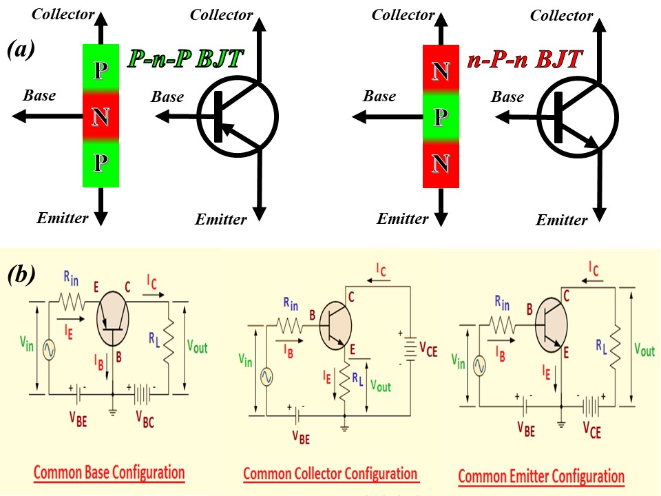
BJTs are classified into two groups based on their nature and structure as shown in Fig. 1(a). The BJTs can be divided into two types
a) NPN
b) PNP
NPN BJT
A P-doped layer of semiconductor exists between the two layers of n-doped material in an NPN (negative-positive-negative) BJT. The base of the transistors is represented by the P doped region, while the emitter and collector are represented by the other two layers.
Because minority charge carriers on the base side are utilized to control significant current at the transistor’s other terminals, NPN transistors are also known as minority carrier devices. On the base side, electrons operate as a minority carrier while the current flows from an emitter to a collector.
PNP BJT
The PNP (positive-negative-positive) transistor is a form of BJT in which a base layer of N doped semiconductor is sandwiched between two layers of P doped material. To regulate a big current at the emitter and collector sides, the base utilizes a lower base current and a negative base voltage, and the voltage at the collector side is greater than the voltage at the base side. When compared to NPN transistors, the current and voltage polarities of PNP transistors are reversed.
PNP transistors act similarly to NPN transistors, with the exception that holes from the emitter are diffused through the base and collected by the collector. Conduction current produced by the movement of electrons is deemed rapid and has more value than conduction current produced by the movement of holes, hence this transistor is rarely employed for applications.
Working of a Bipolar Junction Transistor
BJT has different regions of operation.
Forward Active Mode
The emitter-base junction and the collector-base junction are the two types of junctions found in BJTs. The collector-base junction is reverse biased, while the emitter-base junction is forward biased.
Most transistors have a high common-emitter current gain for amplification, which shows the exact current and power gain required for amplification. The collector-emitter current is mostly determined by the base current, which is used to manage the enormous currents flowing through the emitter and collector.
Reverse Active Mode
Transistor switches from active to reverse active state by swapping the emitter and collector. Most transistors are built to have a high current gain, but reversing the role of the emitter and collector reduces the current gain significantly when compared to the forward-biased area. Unless a failsafe condition is necessary, this mode is rarely employed.
Saturation Mode
When both junctions are forward biased, the BJT enters saturation mode. This is referred to be a closed circuit because it permits a considerable quantity of current to flow from the emitter side into the collector side.
Cut-off
When the emitter-base junction is not forward biased, the transistor is said to be in the cut-off zone, where the collector and base currents are zero regardless of the voltage supplied to the base terminal.
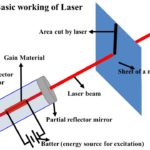
Basic configurations of a Bipolar Junction Transistor
BJT (bipolar junction transistor) is a current-controlled device that is mostly used for amplification and switching. This gadget can be connected to external electronic circuits in three ways also shown in Fig. 1(b).
- Common Base
- Common Collector
- Common Emitter
For different setups, the nature of the current controlled at the output varies.
Common base
The common base is shared by the input and output signals in a common base arrangement.
At the emitter-base junction, a voltage is supplied, and the equivalent output signal is obtained at the output across the base-collector junction.
The base voltage is connected to a reference voltage or, in certain circumstances, grounded, with the goal of creating a common base between the input and output signals.
Common collector
The input is applied at the base terminal, and the output is drawn from the emitter terminal in this type of common collector configuration, also known as a voltage follower.
Because the input impedance of this design is extremely high and the output impedance is extremely low, it is mostly utilized for impedance matching.
Non-inverting amplifiers have a common collector arrangement in which the output signal and the input signal are in phase
Because the load resistance lies at the receiving end of both collector and base currents, this transistor has a very high current gain, making it ideal for amplification. As a result, even a small voltage gain (around unity) can assist produce a high current gain.
Common emitter
In a transistor-based amplifier, an input signal is applied between the emitter and the base, while the output is derived from the emitter and the collector.
This combination has the maximum current and power gain, making it an excellent amplification option. The input impedance is connected to a forward-biased PN junction that has a low value, whereas the output impedance is coupled to a reverse-biased PN junction that has a high value.
The common emitter arrangement is used in the majority of transistors because it provides the appropriate power and current for amplification.
Inverting amplifier circuits have a common emitter layout where the input signal is out of phase with the output signal.
Applications of Bipolar Junction Transistors
Amplification and switching are the two main applications of BJTs.They serve as the foundation for most electrical circuits, particularly where audio, current, or voltage amplification is necessary.
For amplification, NPN transistors are favored over PNP transistors because conduction through electron mobility is better than conduction through the hole mobility.
Further readings
If you liked this post, you might be interested in reading the following posts.
- Laser and its applications in medicine and technology
- Birefringence and birefringent materials

- Blackbody radiation calculator for specific wavelengths and temperatures
- Light Emitting Diodes (LEDs), their design and applications
- Design of MOSFETs, their working, and applications
- Construction, working, and new technologies of OLED TV
- Laser and its applications in medicine and technology
- LED light, its construction, types and colors, power, life, and technology
- Optical fiber design and applications
- Radiation therapy for cancer treatment and its side effects
- X-ray Imaging: What are X-rays and how are X-ray images taken?
- Scattering of light and its different types
- The achromatic lens to remove chromatic aberration
- Wave plates and polarizers for polarization manipulation
- Birefringence and birefringent materials
- Demystifying Solar Panel Specifications: Your Guide
- Construction, working, and new technologies of OLED TV
- LED light, its construction, types and colors, power, life, and technology
- Latest Trends And Development In Solar Technology
- Geothermal energy and its advantages
- Solar tracker to increase the efficiency of solar energy systems
- Solar tree for compact energy collection
- Water pumping system design calculator using solar energy
- Effective harnessing solar energy through spray-on solar cells
- Are perovskite solar cells future of solar energy harvesting?
Oh my goodness! Incredible article dude! Thank you, However I am going through problems with your RSS. I don’t know why I cannot join it. Is there anybody else getting similar RSS issues? Anyone who knows the answer can you kindly respond? Thanx!!
Thanks! Loads of info!