
What is a solar cell?
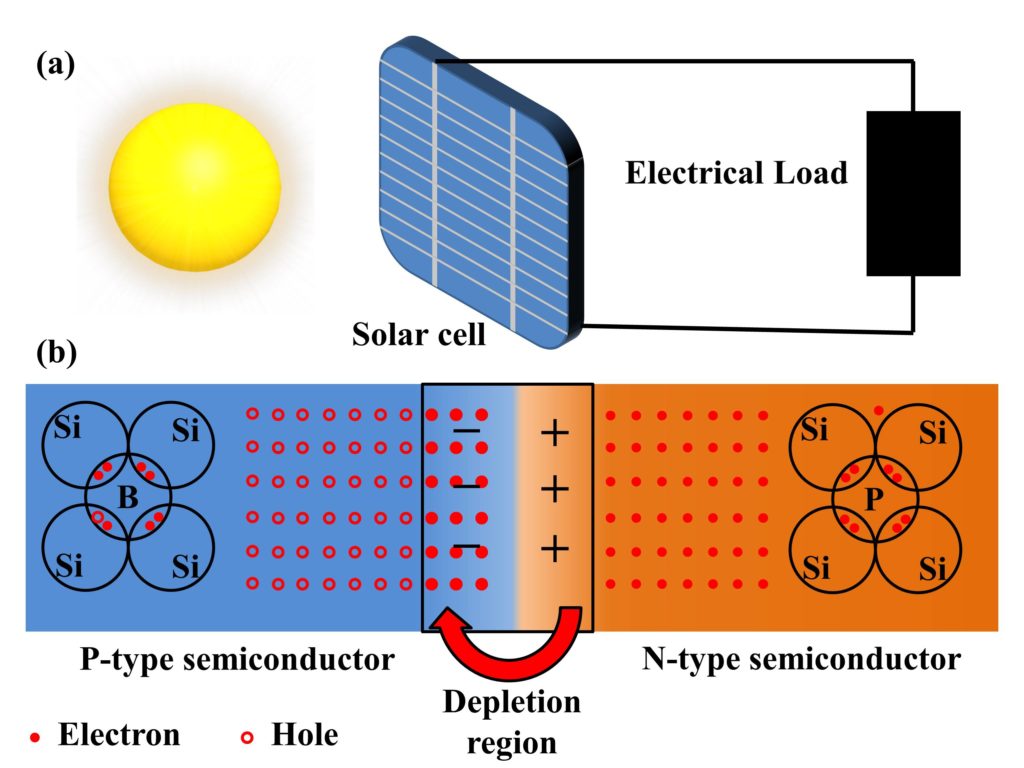
A solar cell is a device that converts solar energy into electrical energy through a photovoltaic effect. This is why a solar cell is referred to as a photovoltaic (PV) cell. The term Photovoltaic effect signifies the generation of voltage and current when photons are absorbed in the solar cell. The conversion of solar energy through the solar cell is shown in Fig. 1(a).
Construction of a Solar cell
A solar cell is made from a p-n junction. A p-n junction is a combination of p-type semiconductor material and an n-type semiconductor material. The p in the p-n junction refers to the positive side of the semiconductor having an excess concentration of holes, and the n of the p-n junction refers to the negative side of the semiconductor that has a higher concentration of electrons. In a semiconductor, the p-n junction is created by the method of doping.
Let’s consider a Si atom with four electrons in its outermost shell. It forms covalent bonds with its neighboring Si atoms. In a p-type semiconductor material, the semiconductor (for instance, Silicon-Si) is doped with impurity from group III elements of the periodic table, such as boron. When Si is doped with impurity from group III elements in the periodic table, holes are formed due to the shortage of one shared electron. Similarly, in an n-type semiconductor material, the semiconductor is doped with impurity from group V elements in the periodic table (for instance, phosphorous-P). When Si is doped with phosphorous, excess electrons are created that can move freely. Both electrons and holes are mobile carriers and contribute to electric current.
When n-type and p-type materials are combined, some electrons from n-type material diffuse in p-type material, leaving a net positive charge on the n-type material side. These electrons move into p-type material and combine with holes, which leaves a negative charge on the p-type side. This charged space created at the center of p-n material stops further diffusion of electrons from n-type semiconductor towards p-type semiconductor and is known as depletion region. A visual depiction of the p-n junction and depletion region is shown in Fig. 1(b).
Working of a Solar cell
In order for a solar cell to generate electricity, a photon having energy greater than the bandgap of a semiconductor material (from which p-n junction is made) is needed. This photon is absorbed by electrons in the valence band, which then move into the conduction band to conduct electric current. For the case of Silicon having a bandgap of 1.12 eV, photons having energy equal to or more than 1.12 eV are required. To elaborate this concept further, let’s convert this energy into wavelength or frequency, and to do that, we can use the formula given below.
where E is energy in eV and λ is wavelength in nm. The wavelength comes out to be 1107 nm for Silicon. Since frequency is inversely proportional to wavelength from v=fλ, lower wavelengths carry more energy since they have a larger frequency. Therefore, for Silicon, electromagnetic (EM) or light waves with a wavelength of 1107 nm and shorter will contribute towards effective electron-hole pair generation. Similarly, for gallium-phosphide (GaP) and gallium-arsenide (GaAs), these values come out to be 554 nm and 860 nm, respectively, for the corresponding bandgaps of 2.24 eV and 1.441 eV. Therefore, GaP will absorb EM waves with wavelengths at or before 554, GaAs at or before 860, and Si will absorb the most solar spectrum up until 1107 nm, as shown in Fig. 2(a).

Direct and indirect bandgap materials
Direct bandgap material is such that its electrons only require a photon (having more energy than the material’s bandgap) to jump from valence band to conduction band. A visual depiction of this concept is shown with the help of E (energy) and k (momentum) diagrams in Fig. 2(b). An indirect bandgap material is shown on the right side of this figure, where an electron requires a photon and a phonon (represents thermal energy or atom’s vibration) to move from the valence band to the conduction band.
Further readings
If you liked reading this post, we suggest reading the following posts that are closely related to “Solar cells, their construction, and working”.

Wonderful post! We are linking to this great content on our site. Keep up the good writing.